
Latest Products


Contact Us
- No.31 Xianghong Road, Xiang'an Distrcit, Xiamen City, Fujian Province, China
- echo-wang@eahunt.com
- +86-592-7616732
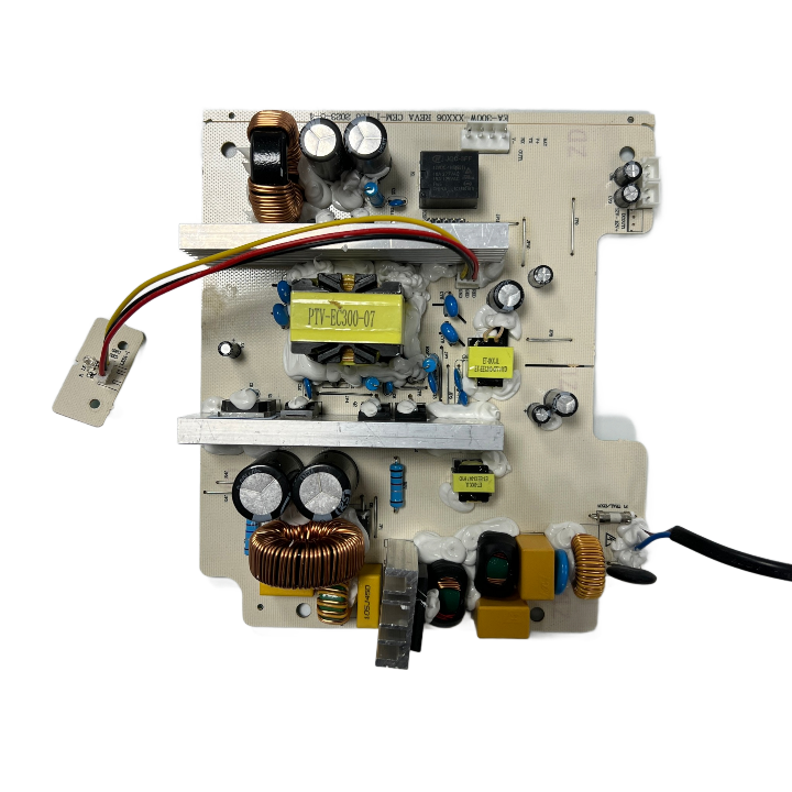
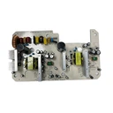
Power Supply Board
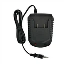
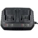
A charger is a common charging device that converts electrical energy into DC energy and outputs the electrical energy to electronic devices such as cell phones, tablets, digital cameras, etc. through a USB cable that connects the charger to the electronic device, thus enabling the charging process. The charger does not require the use of a computer or other device to charge, it simply needs to be plugged into a wall outlet.
Description

Circuit board production process:
1、Cutting
The original copper-clad board will be cut into a process that can be used in the production line to produce the board
2、Drilling
Make PCB board layers to produce through-holes to connect between layers.
3、Sink copper
After drilling the circuit board in the copper sink cylinder will occur in the redox reaction, the formation of copper layer on the hole for hole metallization, so that the original insulated substrate surface deposited on copper, to achieve the electrical interlayer communication.
4、Pressing film
After pressing the PCB board is pressed with a layer of blue dry film, dry film is a carrier, in the circuit process is very important. Compared with the wet film, the dry film has higher stability and better quality.
Can directly do non-metallic over-hole.
5、Exposure
The negative and pressed dry film substrate alignment, the use of ultraviolet light exposure machine, the negative graphics transfer to the light-sensitive dry film.
6、Developing
Use the weak alkaline developer to develop the dry film or wet film has not been exposed to dissolve and rinse off, retaining the exposed part.
7、Electric copper
The pcb board into the electric copper equipment, copper part of the electricity on the copper, the dry film blocked part of the reaction is not!
8, electric tin
The purpose is to remove that part of the copper protected by the dry film to do the preparatory work.
9、Elimination film
Will protect the copper surface has been exposed to the dry film with sodium hydroxide solution stripped off, revealing the line graphics.
10, etching
Has not been exposed to the dry film or wet film is removed by the developer will reveal the copper surface, using acidic copper chloride to dissolve this part of the exposed copper surface corrosion off, to get the desired line.
11、Tinning
Tin retreat is used to retreat the tin water on the line, so that the line back to the original color of copper.
12、Optical detection
There are two general detection methods, one is to observe with the naked eye, the second is the use of optical AOI. AOI working principle is to first use high-definition image camera for rapid shooting, and then use the picture taken with the original file for comparison, can fundamentally solve the open short circuit, and micro open, micro short and other hidden problems occur.
13、Print solder resist oil
Solder resist is one of the most critical processes in the production of printed circuit boards, mainly through screen printing or coated with solder resist ink, coated with a layer of solder resist on the surface of the board, through exposure development, to reveal the disk and holes to be soldered, other places covered with a solder resist layer to prevent short circuits when soldering
14, solder resist exposure, development
The purpose is to remove the solder resist oil from the pads and other places. First, the solder resist film on all covered with green oil on the board, film (to open the window where the black, do not open the window where the transparent), and then put on the exposure machine for exposure, to open the window part, because the film is black, black blocked the light is not exposed, with the state of the solder resist green oil changed, part of the green oil is exposed, part of the green oil is not exposed, from the surface to see, at this time or green.
15、Character
The required text, trademarks, parts and other symbols, printed on the PCB board surface in the form of screen printing, and then exposed to ultraviolet radiation on the board surface
16、Surface treatment
The purpose is to ensure good solderability or electrical properties. Common surface treatment: spray tin, sink gold, OSP, sink tin, sink silver, nickel-palladium gold, electric hard gold, electric gold finger, etc.
17、Forming
Cut the PCB into the required form factor.
18、Electrical testing
Simulate the state of the circuit board, power on to check the electrical properties for open and short circuit.
19、Final inspection, sample test, packaging
Check the appearance, size, aperture, thickness and mark of the board to meet customer requirements. The qualified products will be packaged for easy storage and transportation.
tel: +86-13860786068
Envelope: athene-cai@eahunt.com
Address:No. 31, Xianghong Road, Xiang'an Industrial Zone, Xiamen Torch High-tech Zone, XIAMEN, Fujian 361101
Whatsapp: +86-13860786068
Wechat: Athene225
Hot Tags: power supply board, China, suppliers, factory, customized, price, for sale, 12v dc to 12v ac 50hz, asian power devices inc ac adapter, usb power adapter for laptop, battery powered portable charger, 20v 2.25 a charger, 45w charger type c
You Might Also Like


